SKC Actively Launches Chemical Mechanical Polishing (CMP) Pad Business
(Materials for polishing semicon wafer)
● SKC’s readies CMP pad mass production facility and obtains certification from local customers
● Sales of 300 billion won targeted in 2025 with fully integrated production system ranging from raw materials to finished products
● World-class competitive advantage secured in wafer CMP materials market with synergy and CMP Slurry business
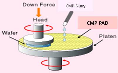
Just one year after declaring its launch, SKC (Lee Wan-jae, CEO) has finally launched its CMP pad business after obtaining the required product certifications from global semicon producers, and its mass production facility in Korea. Chemical Mechanical Polishing (CMP) pads are high value-added polyurethane products that are used to level semicon wafers by polishing the surface. The world market has so far been monopolized by a US-_ base_d global supplier with high barriers to market entry, including patent. SKC was able to launch the CMP pad business by acquiring CMP pad patents and business rights from Dong sung A&T in September of last year.
CMP pad factory with annual capacity of 50,000 sheets built at Yongwol Industrial Park, Anseong, Gyeonggi-do
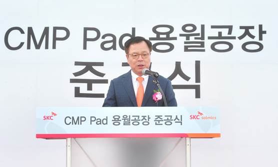
SKC held a ceremony to celebrate the construction of its CMP pad factory at Yongwol Industrial Park in Anseong-si, Gyeonggi-do, with Lee Wan-jae, SKC CEO, Gwon Hyeok-jin, chair of Anseong-si Council, Han Yeong-se, chair of the Anseong Industrial Park Management Corporation, and over 100 guests from home and abroad in attendance. SKC has built the CMP pad factory, which has an annual production capacity of 50,000 sheets, on a 5,680m2 plot of land at Yongwol Industrial Park, investing 20 billion won in the nine months since its commencement in December of last year. “We will contribute to the localization of semicon chip materials with the ultimate goal of developing a core material pre-polymer in house, securing technologies for the mass production of pads, and increasing the sales of our CMP slurry materials in order to secure a competitive business _ base_ in the semicon chip materials market, which is heavily controlled by foreign businesses,” declared SKC CEO Wan-jae Lee in his congratulatory speech.
Company acquires pad product certification from global semicon makers in Korea, applies key processes starting in October
SKC has disclosed that it recently obtained certification from a global semicon chip maker of pads used in key processes, including the W process of DRAM and Flash devices, and that the pads will be applied to the customer’s process in October. It is significant as the locally developed product is now being applied to key processes in the CMP pad market, which has a high entry barrier. According to industry experts the integrated production system capable of producing world-class products has great appeal for customers. The integrated production system was developed by securing patented technologies related to pads, producing the raw materials required for CMP pads at an existing chemical line, and combining the relevant technological capabilities _ base_d on a strategy of aggressive project implementation. He also explained that “As SKC is fully equipped to develop and produce core pad materials pre-polymer and finished products, it is able to supply products customized to customers’ diverse requirements at competitive prices.”
Company targets 300 billion won in sales and 30% of world CMP pad market by 2025
The CMP pad is a highly functional, high value-added polyurethane product that required incessant technology innovation. SKC plans to increase its sales to 300 billion won (30% of the global market) by 2025 by investing 50 billion won in its CMP pad line by 2020. In addition, it is expected to secure world-class competitiveness in the semicon CMP pad materials market as it is set to commercialize CMP slurry, the chemical material used in the CMP process along with CMP pads - through the development and mass production of CMP slurry.
[End]
Reference materials
1. Chemical Mechanical Polishing (CMP) pad
- A consumable polyurethane-family material that is used to level a semicon wafer surface during the wafer CMP process along with CMP slurry by polishing it with a physical and chemical reaction. It is produced by mixing pre-polymer with a hardener and a blowing agent.
* Pre-polymer accounts for a large percentage of the cost of producing CMP pads. SKC is equipped with the pre-polymer R&D and production facilities etc.
2. CMP process
-The process of applying mechanical and chemical force to the surface of a body of water in order to level it through a combination of CMP slurry and a pad.

3. CMP slurry
- A colloidal suspension chemical material with abradants mixed to level the wafer surface during the CMP process by a physical and chemical reaction along with CMP pad. It peels off the wafer surface through chemical reaction with insulated membrane SiO2. The CMP process should be stopped at the desired step depending on the composition of the chemical materials.
[Photo de ion]
1) Photo of ceremony dedicating the SKC CMP pad factory built at Yongwol Industrial Park

2) Profile photo of Lee Wan-jae, SKC CEO

3) Photo of SKC CMP pad
- CMP pad for 300mm wafer developed by SKC
4) SKC logo

