NEWS
SKC, announces the world’s first commercialization of glass substrate: a game changer for semiconductor packaging
2021-10-28
Data processing improved greatly while power consumption is reduced
followed by tech certification by a global semiconductor manufacturerSKC to build a 12,000-square-meter production plant in Georgia, U.S. by
2023 and target to expand it into a 72,000-square-meter production plant by
2025
SKC (CEO Lee Wan-jae) is starting to commercialize high-performance computing glass substrate that it has developed for the first time in the world. Glass substrate is a futuristic material that is considered a 'game changer' in the semiconductor packaging field because it can significantly increase the performance and power efficiency of computer chipsets.
SKC held a board meeting on the 28th and decided to build a semiconductor glass substrate production _ base_ within the premises of SKC inc. in Georgia, USA by investing a total of US$80 million, including a technology value of US$70 million. It is aiming to complete the 12,000-square-meter mass production facilities by 2023.
SKC's glass substrate for high performance computing (HPC) is expected to change the game for semiconductor packages. When a glass substrate is applied, the package thickness is cut in half and so is power consumption. Data center footprint can be significantly reduced as data throughput is dramatically improved. The company’s prototype has already been certified technologically by a global semiconductor manufacturer.
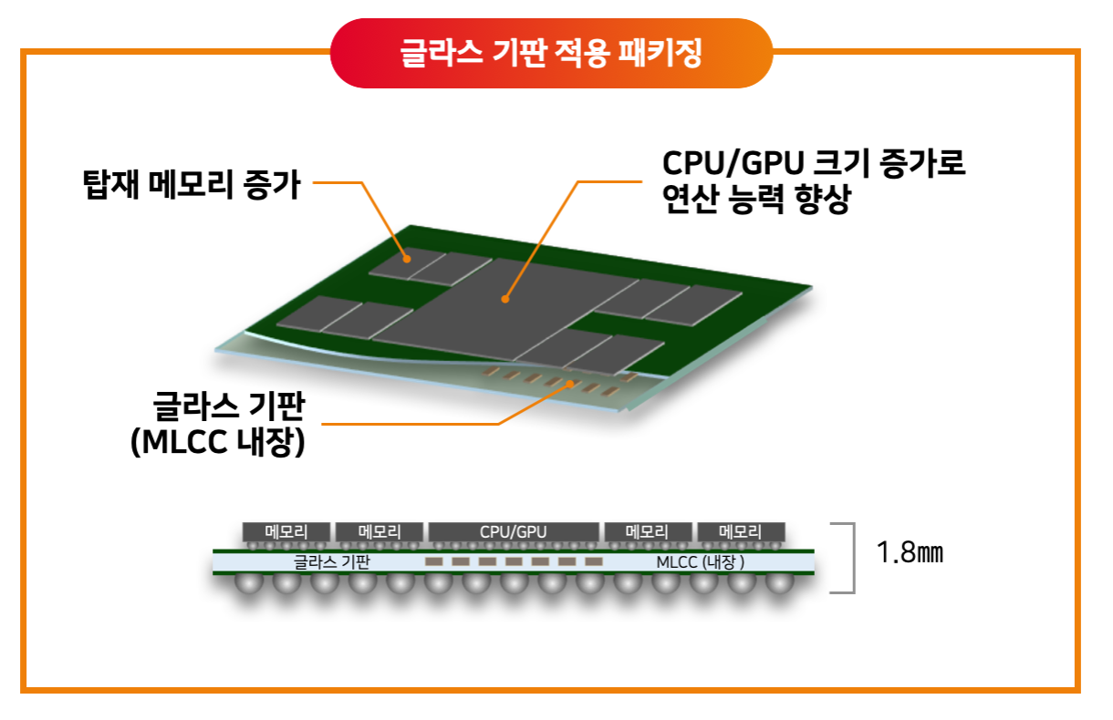
In general, semiconductors such as CPU, GPU, and memory are packaged as one component on a substrate together with several MLCCs before being connected to a PCB. Plastic substrates were widely used, but their uneven surface turned problematic for high-performance semiconductor packaging involving repetitive miniaturization. An alternative method was developed in which silicon with a smooth surface was used as an intermediate substrate(interposer).
However, compared to a glass substrate, this method has low efficiency and limited uses; The package gets thicker due to an interposer, making it hard to be used for mobile applications; The increased distance between the semiconductor chip and the PCB results in larger power consumption, too. In addition, it is difficult to economically produce large-area rectangular substrates required for high performance in round silicon.
By contrast, the SKC glass substrate has a smooth surface and can make a large square panel, so it can respond to the trend of larger size products as well as the miniaturization of semiconductor packaging. The glass substrate does not require an interposer, reducing its thickness and raising its power efficiency. So it can be applied to mobile products easily. It is particularly advantageous for high performance products as MLCC, which had to be installed on the surface of the board, can be placed inside the board so that larger CPUs or GPUs can be mounted on the surface with more memory when necessary.
SKC has decided to consider expanding the production capacity to 72,000 square meters per year by 2025, given that the semiconductor packaging market for high-performance computing is rapidly growing due to a surge in data throughput such as AI and data center servers. According to multiple market research institutes, the market will nearly triple from US$3.5 billion in 2020 to US$9.7 billion in 2025.
An SKC official said, "SKC's glass substrates are receiving great attention from global semiconductor material suppliers and semiconductor manufacturers alike as they are produced with the groundbreaking technology that enables chip designers to achieve the maximum performance they can ever aspire to,” adding, “We will build a stable business _ base_ in collaboration with our business partners so we supply our innovative products to global semiconductor manufacturers while contributing to innovations across the industry using high-performance semiconductors.”
[Reference
photo]

[The glass
substrate for semiconductor packaging developed by SKC for the first time in
the world. It is called the ‘game changer’ in the field of semiconductor
packaging due to its thin thickness leading to high power efficiency on top of
its outstanding data processing performance.]
[The packaging
with a glass substrate developed by SKC for semiconductor packaging for the
first time in the world.]
SK-C Tower, 15 Chungmu-ro, Jung-gu, Seoul, Republic of Korea TEL: 02-3787-1234

Copyright by SKC. All rights reserved.